A Circularly Polarized 1 Bit Electronically Reconfigurable Reflectarray Based on Electromagnetic Element Rotation
IEEE TAP, vol. 69, no. 9, pp. 5585–5595, Sept. 2021
圆极化可重构反射阵以前有条死路:相位靠「转单元」给(Huang 1998),电控就得把旋转对称做出来,管子少不了。文献里唯一做成二维扫描的 CP 阵 [13],一个单元四只管。管子多 → 偏置烦、损耗大、难做大阵。
这篇的骚操作一句话:别真转,也别为了假装转去保留旋转对称。圆贴片基模的场本来就有对称性——把关断的那只管挪到中心对称点,对基模几乎没感觉。所以两只管对调通断 = 虚转 90° = CP 相位翻 180°。只要线对称,二极管砍半。
结果:16×16 实物,峰值 21.8 dBic,口径效率 20%,镜面交叉极化约 −18 dB;2-D 扫描前向增益起伏 <2 dB。通讯作者 Fan Wu,东南大学毫米波实验室。你库里的 [[P18]] 就是在这个 trick 后面加一圈延时线,把 1-bit 虚旋转做成多比特。
这是 11 页 TAP,按处方读,不必逐字通关:
| 节 | 强度 | 这块干什么 |
|---|---|---|
| 摘要 + I | 🔬 精读 | 卡点:电控旋转必须旋转对称 → 管子多 |
| II 开场 + II-A | 🔬 精读 | 一只管先把单元做成 CP(Huang 条件) |
| II-B Fig.6–7 | 🔬 精读 | 全文题眼:对调通断 = 虚转 90° |
| Fig.8–10 + III | 🧭 选读 | 斜入射/焊偏 + LED 看状态 |
| IV-A | 🧭 选读 | 21.8 dBic / 20% / 作者认栽 T2 |
| IV-B + Table III | 🔬 精读 | 扫描兑现,对比四管方案 |
| V | ⏭️ 跳过 | 摘要复读 |
1. 引言:电控旋转太贵了精读约 12 分钟
Abstract—A circularly polarized (CP) reflectarray with 2-D electronically steerable beam is reported. The reconfigurable CP reflectarray element is realized using a circular-patch-based structure with p-i-n diodes incorporated. A new electronical phase manipulation method is proposed based on the element rotation technique and by additionally exploiting symmetries in the field distribution of the element's fundamental resonant mode. Element rotation can be equivalently achieved by altering the biasing voltage and changing the electromagnetic behavior of the reflective phasing cell. The proposed design approach brings about simplification in element configuration, leading to a reduction in the number of required diodes by a factor of one half. Practical concerns of the element and biasing complexity as well as the insertion loss are, therefore, well-handled. A fully functional 16 × 16 reconfigurable CP reflectarray is designed, fabricated, and tested to validate the concept. Good beam focusing and 2-D dynamic beam steering capabilities are confirmed through experiments, along with decent polarization purity and comparatively high aperture efficiency. The proposed simple and robust design could be attractive for implementing lightweight, low-cost, and large-scale 2-D reconfigurable CP reflectarrays.
HIGH-GAIN antennas with their focused beam being able to be dynamically redirected to other intended directions, that is, beam steering capability, can be of practical use to improve the performance of wireless systems such as the next-generation wireless communications, remote sensing, and satellite communications. Conventional aperture antennas including parabolic reflector antennas and phased arrays provide a classical and easy comprehensive way to achieve high antenna gain. However, the drawback associated with the reflector antenna is that beam steering with good performance should be achieved through mechanical tuning. As for the phased array, digitally controlled phase shifters are incorporated to adjust the radiation phase of each array element, which tremendously increases the complexity, fabrication cost, and physical volume of the antenna.
Reflectarray has been considered as a promising alternative for high-gain antenna since it combines feasible features from both the reflector and phased array [1]. It shows the flexibility of scanning the beam by designing different phase compensation scheme while preserving the simple spatial feeding configuration and eliminating the need for complex and lossy feed network. Reconfigurable reflectarrays with dynamic beam control have received widespread research attention during the past decade [2]. The incorporation of discrete elements such as varactor diodes, p-i-n diode switches, and MEMS switches within the unit cell allows the element to change their resonance, scattering behavior, and the reflection phase. Adaptive beam steering can therefore be achieved in a fast, reliable, and comparatively high-efficiency manner with low cost and relatively simple hardware. For instance, discrete phase manipulations with a resolution of one or several bits are implemented with a single switch or the collaborative operation of several p-i-n/MEMS switches [3]–[5]. Continuous reflection phase change can be obtained using varactor-diode-inserted elements and a linearly adjustable biasing voltage [6]. In addition, tunable materials including liquid crystal, ferroelectric film, and graphene also provide promising solutions for launching reconfigurable beams, especially at higher operating frequencies [2].
Single-bit reconfigurable reflectarrays using p-i-n diode switches are of practical interest due to their simplicity and low cost, though the challenges are also clear, including the decreased aperture efficiency, degraded cross-polarization discrimination (XPD), and possibly higher sidelobe level (SLL). The classical yet efficient design approach, in which the radiating edge of a rectangular patch is shorted to the ground through p-i-n diode so as to switch between two different operation states, has been widely studied and applied to realize various designs achieving linearly polarized, dual-polarized, and/or dual-band operations [7]–[10]. However, few investigations that target at 1 bit circularly polarized (CP) beam steering have been reported for reflectarray design [2], [11], [12]. To the best of the authors' knowledge, only one reported design of fully functional electronically beam steering CP reflectarray can be found in the literature within the antenna and propagation community [13].
To date, most reported mechanical [14] and electronical [13], [15], [16] tuning techniques for achieving reconfigurable CP reflectarray element are rather straightforward extensions based on the element rotation method proposed by Huang and Pogorzelski [17]. They all require the element to be rotated, either physically or geometrically, to adjust the phase. It is not difficult to figure out that in the reported electronical approaches, rotational symmetry in element configuration should be reserved to realize the geometrical rotation in an electronical manner. This places a strong constraint on the element configuration and the minimum number of diodes needed. As a result, the design complexity, fabrication cost and the insertion loss will become the primary concerns. Evidently, 1 bit CP reconfigurable element with new design philosophy that brings about simplification in element configuration and enhancement of efficiency would be desirable, for facilitating the development of large CP reconfigurable reflectarray.
In this work, a single-bit CP electronically reconfigurable reflectarray based on electromagnetic element rotation is proposed. To address the challenge of lowering element complexity and reducing diodes number, symmetries in the field distribution of the fundamental mode of a circular-patch-based structure are exploited, in addition to the element rotation technique, for enabling a new electronical approach of manipulating the phase. Only line symmetry in element configuration is required for the proposed 1 bit CP element, which essentially helps simplify the element and halve the number of diodes. 2-D beam steering capability with high circular polarization purity and improved aperture efficiency are achieved. This article is organized as follows. Section II presents the proposed 1 bit CP reconfigurable element and the operating mechanism. Section III introduces the considerations in design and implementation of the fully functional reconfigurable reflectarray. The measured results of the fabricated prototype are provided and discussed in Section IV. Finally, the conclusion is drawn in Section V.
- element rotation method
- 单元旋转法。Huang 1998:CP 反射相位 = 2×旋转角。机械转或电控几何转都从这儿来。
- rotational symmetry
- 旋转对称。电控『假装转』时,单元转一圈还得长得一样,管子数量被对称阶数锁死。
- line symmetry
- 线对称。这篇只要关于一条轴镜像对称,两只管就够 1-bit。
- XPD
- 交叉极化鉴别度。共极化比交叉极化高多少 dB,CP 纯度的成绩单。本文单元 >15 dB。
2. 先做成 CP:一只管就够精读约 14 分钟
A new reconfigurable reflectarray element that is capable of electronically altering the phase of the backscattered CP wave in 1 bit manner is developed. The configuration of the proposed element is depicted in Fig. 1. The element is designed based on a circular microstrip patch antenna that operates at its fundamental resonant mode. As shown in Fig. 1(b), two shorting pins located symmetrically about the y-axis are placed on the radial lines along the phi = 45° and 135° directions with a specific distance to the patch center. Two p-i-n diode switches (MA4AGP907 from MACOM) oriented parallel to the radial directions are inserted, with their one end soldering onto the patch and the other to the top pad of the pin. The diodes are used to enable or block possible currents that flow into the ground from the patch surface. The connectivity of the pins can, therefore, be controlled by switching on and off the diodes.
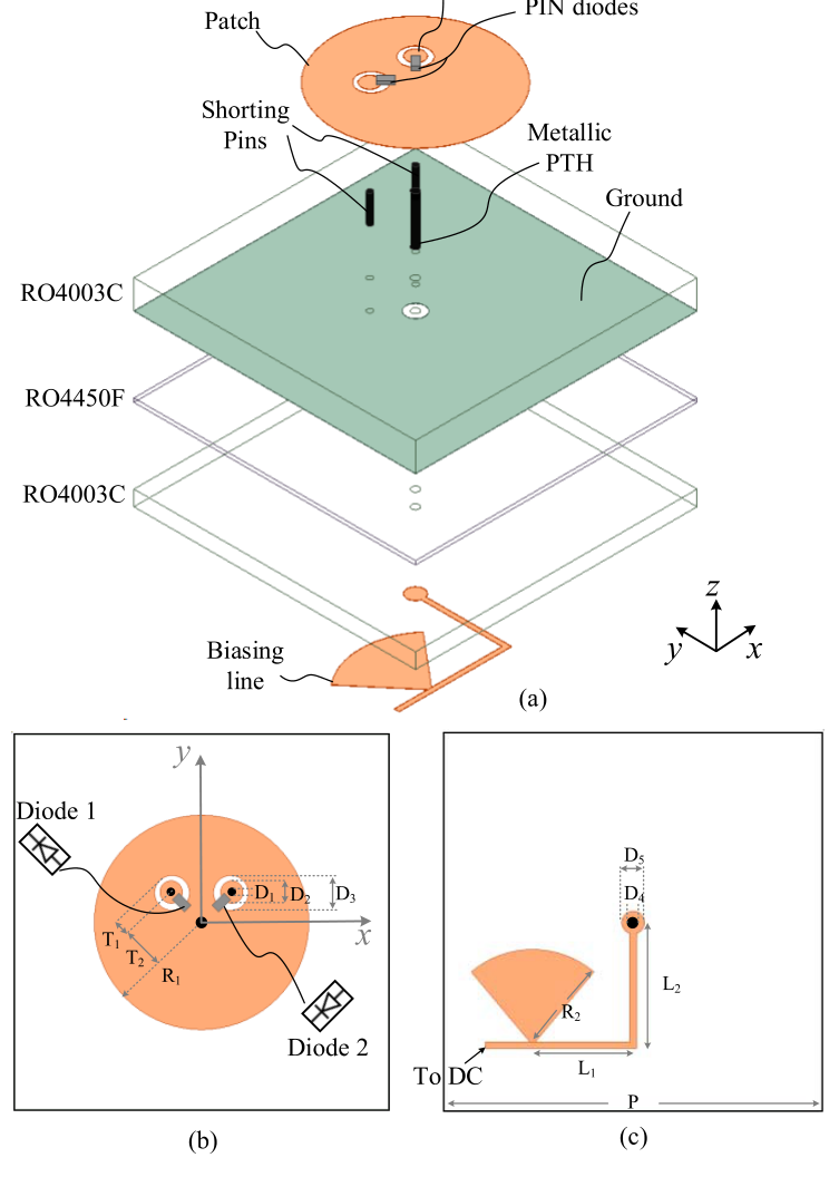
The biasing circuit supplying direct current (dc) voltage is implemented at the opposite side of the ground plane and connected to the patch through a metallized plating through hole (PTH) located at the center of the patch (i.e., the common nodal point of two orthogonally polarized fundamental modes). A band-stop filter composed of an open-circuit stub and a quarter-wavelength microstrip line is adopted to further suppress the radio frequency (RF) signal on the dc line. Dual-layer substrate configuration is used, to accommodate the reflectarray element and the biasing circuit. The patch and the ground plane are realized at the top and bottom sides of the upper substrate while the dc line is designed at the copper layer beneath the lower substrate. The two substrates (RO4003C, dielectric constant of 3.38, thickness of 1.52 mm for the upper one and 0.81 mm for the lower one, respectively) are bonded together using a 0.202 mm thick adhesive film (RO4450F, relatively permittivity of 3.52). The patch, the ground plane, and the dc line are all considered as copper plate with actual thickness. The design procedure of achieving 1 bit CP reconfigurable reflectarray element can be broken down into two parts: the implementation of a CP reflectarray element and the realization of 1 bit electronical phase control. The method and principle of achieving CP operation and electronical phase manipulation will be, respectively, explained.
Consider the case when only one of the two diodes is switched on for electrically connecting the shorting pin to the patch and let the element be illuminated by a left-hand CP incident wave propagating in the −z-direction. According to Huang's analysis in [17], a CP reflectarray element can be achieved when the reflection phase of one LP component differs by 180° from that of the orthogonal LP component. On the other hand, it has been suggested in the classic patch antenna design [18], [19] that shorting pin if placed at the nonnull point of the electric field can affect the resonant frequency of the corresponding mode. Reflection phase difference is then expected to be between the 45°-polarized and 135°-polarized LP components since the two diode-controlled shorting pins, in this case, will result in different resonant frequencies for the two orthogonally polarized fundamental modes. Moreover, the difference in reflection phase can be tuned by changing the distance between the pin and the center of the patch. Consequently, a CP reflectarray element can be properly designed when only one of the diodes is turned on and appropriate geometrical specifications are selected to secure the required 180° reflection phase difference between two orthogonal LP components.
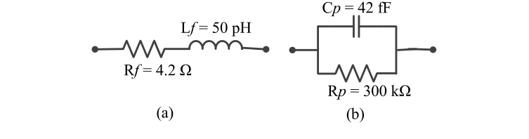
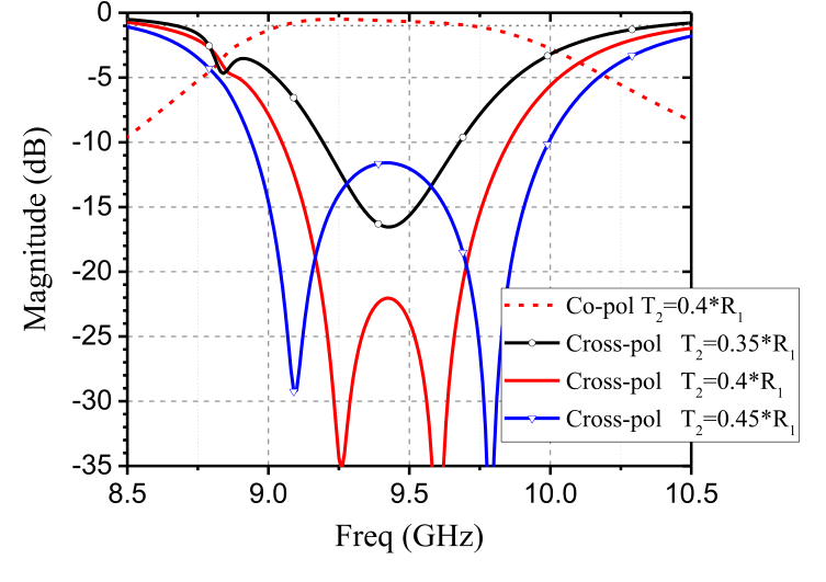
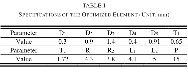
The CP performance of the element under oblique incidence (in line with the off-set angle of the feed horn described in Section III) is simulated in full-wave electromagnetic software Ansys HFSS using floquet mode excitation and periodic boundary condition. Two equivalent circuits, as sketched in Fig. 2, are adopted to, respectively, model the diode in “ON” and “OFF” states. The simulated results displayed in Fig. 3 shows how the change in pin location affects element CP performance. Optimized performance with geometrical specifications listed in Table I are denoted by the red (dashed and solid) lines in Fig. 3. The optimized design exhibits an XPD of more than 15 dB within the frequency range from 9.1 to 9.8 GHz. The insertion loss is smaller than 1 dB over the operating bandwidth with the lowest value of 0.5 dB found at 9.25 GHz. This demonstrates that the design can be used as a CP reflectarray element with a low insertion loss.
To better support our explanations, field distributions of the resonant modes and the quantitative analyses regarding the magnitude and phase of the reflected wave are presented in Figs. 4 and 5. The results are obtained from a unit cell illuminated by LP incident wave (i.e., the 45°-polarized and 135°-polarized waves, respectively), since the performance of a CP reflectarray element is essentially controlled by the different resonance, and hence scattering of the element upon two orthogonal LP plane-wave excitations. As can be seen from Fig. 4, the fundamental mode of the circular patch is excited when the element is illuminated by either a 45°-polarized or a 135°-polarized incident wave. Different field intensities can be clearly identified for the two excited fundamental modes, as expected (since different states are preserved for the two diodes: only the diode along the 135°-direction is switched on). The magnitudes and phases of the reflection coefficients for the two orthogonal LP components are plotted in Fig. 5 to quantitatively show the different backscattered fields and clarify the sensitivity study illustrated in Fig. 3.
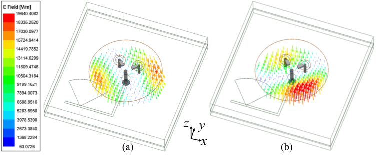
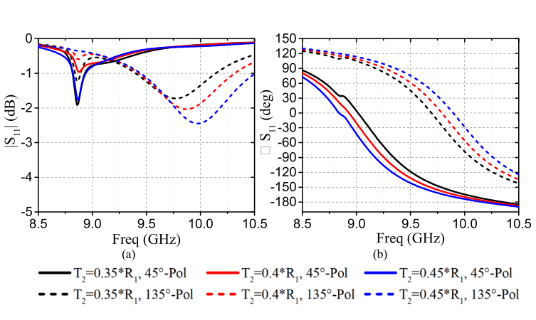
Two observations are found from Fig. 5 which confirm our previous explanations: 1) the activation of only one of the two diodes results in considerably different resonance and backscattered fields for the two orthogonal LP components and 2) the differences in the resonances and backscattered fields can be adjusted by modifying the distance between the pin and the patch center (i.e., T2). In the theoretical analysis of CP reflectarray element by Huang and Pogorzelski [17], losses are neglected and the magnitudes of the two backscattered LP components are assumed to be the same. With p-i-n diodes inserted in the proposed reconfigurable design, the potential imbalance in magnitudes of the two components should be considered, as indicated in Fig. 5(a). Nevertheless, desired CP backscattered wave with the axial ratio (AR) smaller than 3 dB (or XPD higher than 15 dB) could still be generated when proper magnitude ratio and phase difference are achieved between the two LP components. As a side note, the lower magnitudes of the reflection coefficients in Fig. 5(a), when compared with those observed from passive reflectarray elements, are caused by the ohmic losses contributed by the p-i-n diodes. Widest AR bandwidth is obtained when T2 = 0.4 ∗ R2 according to the results presented in Fig. 3. With reference to Fig. 5, it is noted that the deviation of T2 mainly causes change in the phase difference within the operating frequency range from 9.1 to 9.8 GHz while the magnitude ratio remains comparatively stable. The variation in phase difference would go up to approximately 30°. This explains the increases IN cross-polarization levels in Fig. 3 when T2 ≠ 0.4 ∗ R2.
- Huang's 180° condition
- 两个正交线极化反射相位差 180°,合成才是圆极化。PB / 单元旋转法的共同前提。
- T2
- 短路针到贴片中心的距离。拉开两正交模谐振的旋钮,也是全文最敏感的加工尺寸。
- PTH
- 金属化过孔。这里打在贴片正中,直流进出、射频看两个正交模的公共节点。
3. 虚旋转:对调两只管精读约 12 分钟
As stated in Section I, rotational symmetry in element configuration needs to be reserved in reported electronically reconfigurable CP design [13]. This results in a relatively complex element with quite a few diodes needed. Here, by additionally exploiting symmetry in field distribution of the fundamental resonant mode, the CP phase can be adjusted in 1 bit manner without having the element being rigorously rotated. Only line symmetry in element configuration would be required, which considerably reduces the element complexity (e.g., halve the number of diodes). In the proposed method, element rotation of 90° is equivalently obtained by exchanging the ON/OFF states of the two diodes, that is, turning on the deactivated diode and, at the same time, switching off the forward biased diode. The operating principle can be explained with the help of the element evolution diagram illustrated in Fig. 6.
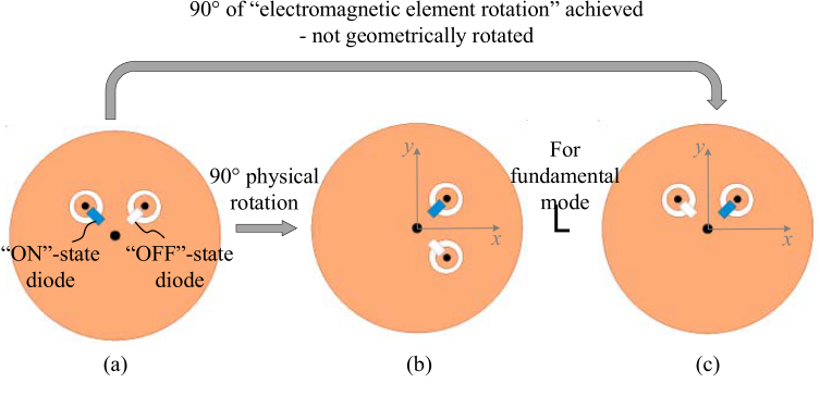
Fig. 6(a) depicts the proposed CP element where only one diode is biased to be in the “ON” state. It is not difficult to understand that a reflection phase change of 180° will be readily achieved if one physically rotates the element with respect to its center by 90°. The rotated element configuration is given in Fig. 6(b). Since the patch operates in the fundamental mode, moving the “OFF”-state diode and the associated shorting pin from the rotated location depicted in Fig. 6(b) to the symmetric position with respect to the patch center, as shown in Fig. 6(c), will not alter the element resonance under 135°-polarized LP wave illumination. The resonance excited by the 45°-polarized LP incident wave is nearly unchanged as well because the “OFF”-state diode and the shorting pin lie always at the nodal line of the corresponding dominant mode. Therefore, the electromagnetic behavior of the element in Fig. 6(c) upon CP wave incidence is almost identical to that of the rotated element shown in Fig. 6(b). Stated in another way, by switching the ON/OFF states of the two diodes, a virtual element rotation of 90° and hence 180° difference in the phase of the reflected copolarization component can be obtained.
To support the claim of simpler element configuration and intuitively compare the proposed method with the reported one, the design of a reconfigurable CP reflectarray element based on the electronical tuning methodology described in [13] is illustrated in Fig. 7, also using the circular-patch-type microstrip element. It can be inferred that the element configuration would be more complex if the design is based solely on the element rotation technique.
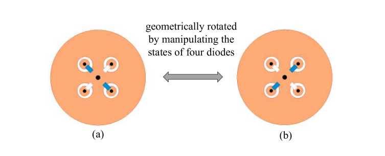
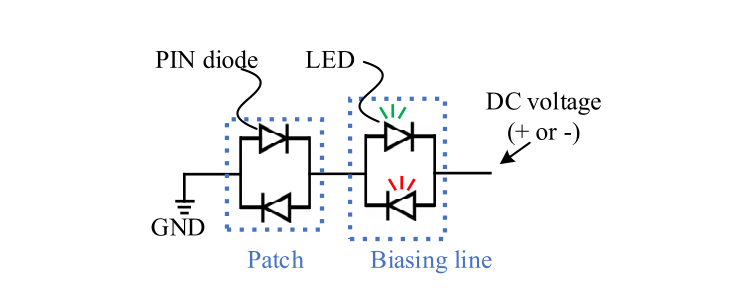
Specifically, with the two diodes designed to have opposite orientations [see Fig. 1(b)] and the ground plane being the reference point for dc voltages, a biasing line that provides either a positive or a negative voltage would be sufficient to control the element state. For easy reference, the biasing voltage, diode state, and reflection phase of the copolarization component for different operation states of the proposed 1 bit CP reconfigurable element are summarized in Table II.
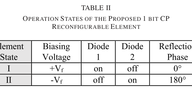
- virtual element rotation
- 虚旋转。不转贴片,用开关改变电流路径,让电磁行为等价于转过某个角度。
- nodal line
- 节线。某个模电场为零的那条线。关断管落在节线上,对这个模几乎透明。
4. 斜入射、焊偏、把阵做出来选读约 10 分钟
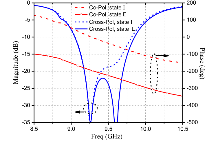
As noted, a stable reflection phase difference of 180° over the operating bandwidth is observed between the two element states while the desired high cross-polarization suppression is well-preserved.
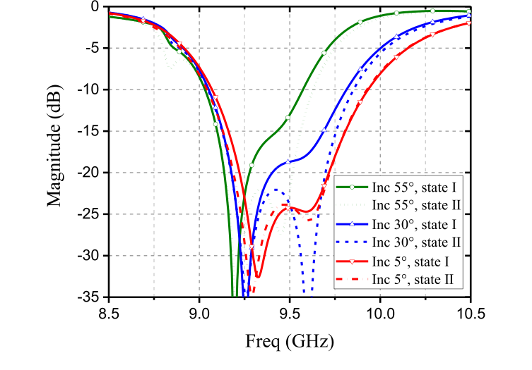
As shown, the cross-polarization level and the operating bandwidth are improved when incident angle decreases from 30° to 5°. The performances are slightly degraded when the incident angle increases to 55°. However, large incident angle only holds true for elements near the edge, and a reported study has already shown that deviation of S-parameters in the edge elements will not have a significant impact on the performance of such space-fed antennas [20].
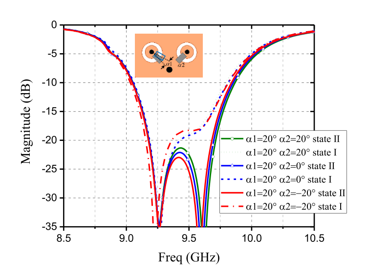
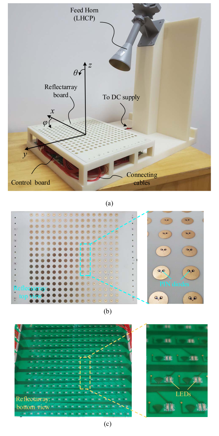
To facilitate debugging and help visually monitoring the operation state of the reconfigurable reflectarray, two light-emitting diodes (LEDs) are added into the dc line of each element, as illustrated in Fig. 11(c). The LEDs are also oriented in opposite directions and connected in parallel. The p-i-n diodes and LEDs are then connected in a series configuration. DC voltage is supplied at one end of the LEDs to power up the diodes and alter the element operation state. The two operation states of the element can be easily distinguished by different LED colors (red or green).
- f/D
- 焦径比。馈源到口径距离 / 口径边长。这里 0.99,边沿约 −10 dB。
- reference phase
- 1-bit 量化时加在补偿相位上的公共偏置。选得好能减小孔径上的平均量化误差,抬口径效率。
5. 镜面实测:数字和认栽选读约 8 分钟
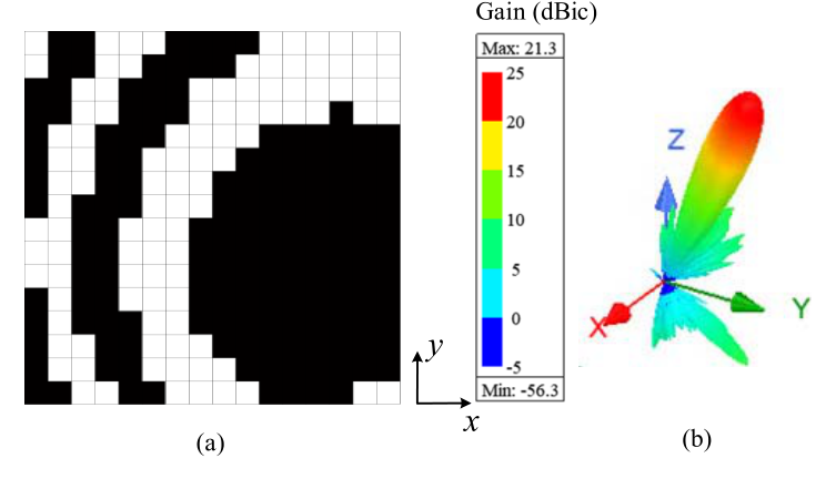
A peak gain of 21.8 dBic and a peak aperture efficiency of 20% are reported. A 3 dB gain bandwidth of 9.4% (9.1–10 GHz) is successfully achieved. In comparison to the simulated 3 dB bandwidth of 7.5% (9.07–9.8 GHz), a measured AR bandwidth of 5.6%, covering frequencies from 9.26 to 9.8 GHz, is observed.
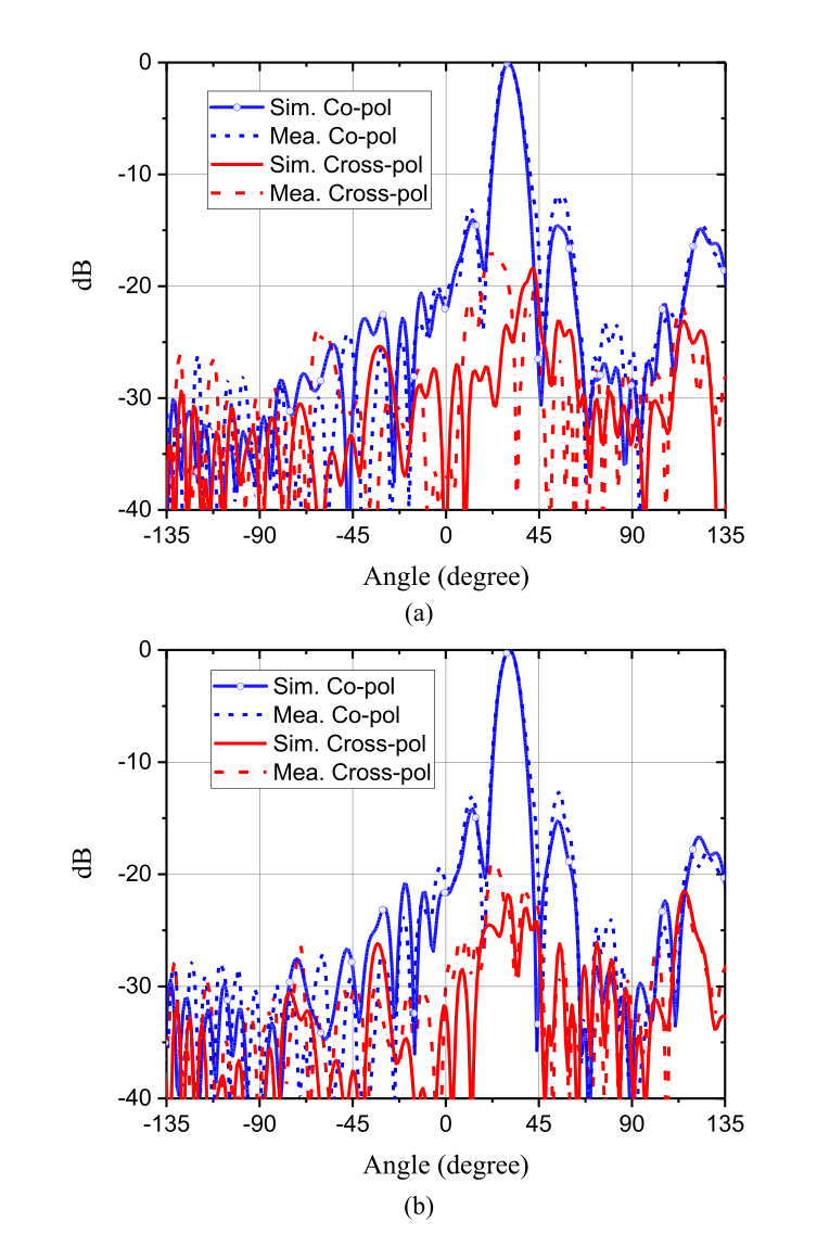
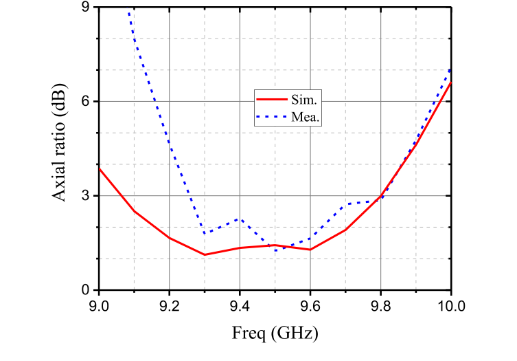
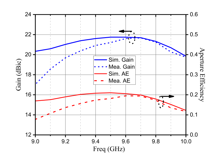
The narrower AR and gain bandwidth are suspected to be caused by the degradation in element bandwidth. Fabrication tolerance (especially for the location of the shorting pins, which has been proven by simulation results in Fig. 3 to be a sensitive parameter controlling element bandwidth) and possible deviation of the p-i-n diode performance under particular temperature, moisture, and biasing conditions from the equivalent circuit model adopted in simulation could be the primary reasons for the element bandwidth degradation.
- specular reflection configuration
- 镜面反射位形。波束指到几何反射方向,口径利用最充分,用来报峰值增益和效率。
- aperture efficiency
- 口径效率。实测峰值 20%。1-bit 量化误差 + PIN 欧姆损耗是主要税。
6. 扫描兑现,管子确实少了一半精读约 12 分钟
The 2-D beam steering functionality is demonstrated by designing and realizing a number of pencil beams with different steering angles in the two main planes. In addition to the radiation patterns revealing the steering capability in the two planes, the antenna gain and AR of the corresponding steering beam are reported in Fig. 17 as well. For beam steering in the phi = 90° plane, high polarization purity is achieved. The measured ARs are well below 2 dB, as displayed in Fig. 17(c). Since this is the plane where the offset feeding horn is situated, feed blockage effect is observed, particularly in the backward beams. The measured results of the forward beams steering from theta = 0° to 45° match well with predictions. A gain variation of smaller than 2 dB is obtained among the forward beams point at different directions. As for the backward beams, a larger gain reduction is found. The gain of the beam steering to theta = −30° is dropped by nearly 5 dB.
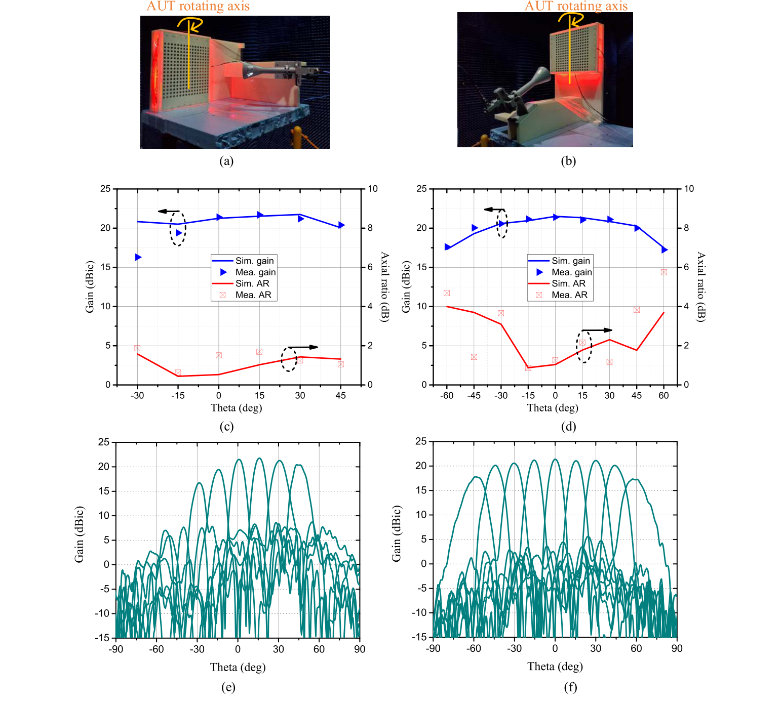
Beam steering in the phi = 0° plane is also considered. The measured antenna gains depicted in Fig. 17(d) are in good agreement with the simulated results, demonstrating a scan loss of no more than 3 dB for beams scanning from −45° to 45°. A relatively small AR is found for beams of steering angles less than 60°. The AR values for the two beams steering to ±60° become larger, mainly due to the drop of copolarization levels. All the measured LHCP radiation patterns in the two orthogonal main planes obtained at the center frequency of 9.5 GHz are plotted in Fig. 17(e) and (f), respectively. The 2-D beam steering capability is well-confirmed and reasonably measured.
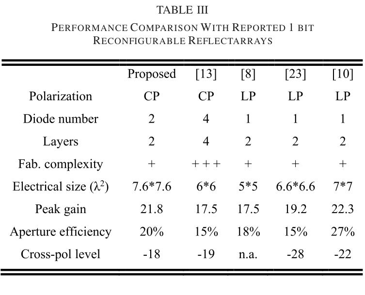
To demonstrate the feasibility of the proposed design, the antenna characteristics are compared with state-of-the-art 1 bit beam-steering reflectarray designs in Table III. Compared with, to the best of the authors' knowledge, the only reported fully functional 2-D electronically beam steering CP reflectarray, the proposed design possesses a much simpler element configuration and requires less diodes to be incorporated. The dual-layer substrate and two-diodes-per-element configuration serve to reduce the complexity to be at about the same level of LP reconfigurable designs. As it is also evidenced, the aperture efficiency of the proposed design is relatively high, comparing to the reflectarray antennas that use a similar number of diodes or perform the same CP beam steering functionality. Degradation in the aperture efficiency of such reconfigurable reflectarrays, when compared with ordinary designs, is primarily caused by the 1 bit phase quantization and the losses introduced by the diodes. It is worthwhile to mention that the proposed design would be able to reconfigure the pattern of the reflected beam with 1 bit phase resolution when the excitation is an RHCP, LHCP, 45°-polarized LP, or 135°-polarized LP incident wave, similar to that shown in [13].
- scan loss
- 扫描损耗。波束离法向越远增益掉多少。本文 φ = 0° 面 ±45° 内 ≤3 dB。
- feed blockage
- 馈源遮挡。偏馈所在面往回扫时,喇叭挡散射,后向 −30° 掉约 5 dB。
7. 结论:摘要复读跳过约 1 分钟
- 回到 Obsidian,打开 [[P05-A Circularly Polarized 1 Bit Electronically Reconfigurable Reflectarray Based on Electromagnetic Element Rotation]],用你自己的话写下:
- 1. Fig. 6 三步里,哪一步是『真旋转』、哪一步是『电磁偷换』?你能不能画给自己看?
- 2. 这篇只要线对称、两只管;[[P18]] 要八边形加一圈延时线。多比特是怎么从『虚转 90°』长出来的?
- 3. 作者把实测 AR 变窄归咎 T2 和二极管模型。你自己做板子时,哪一个更值得在 DFM 里单独控?
- 写完三条,这篇才算真正读完。